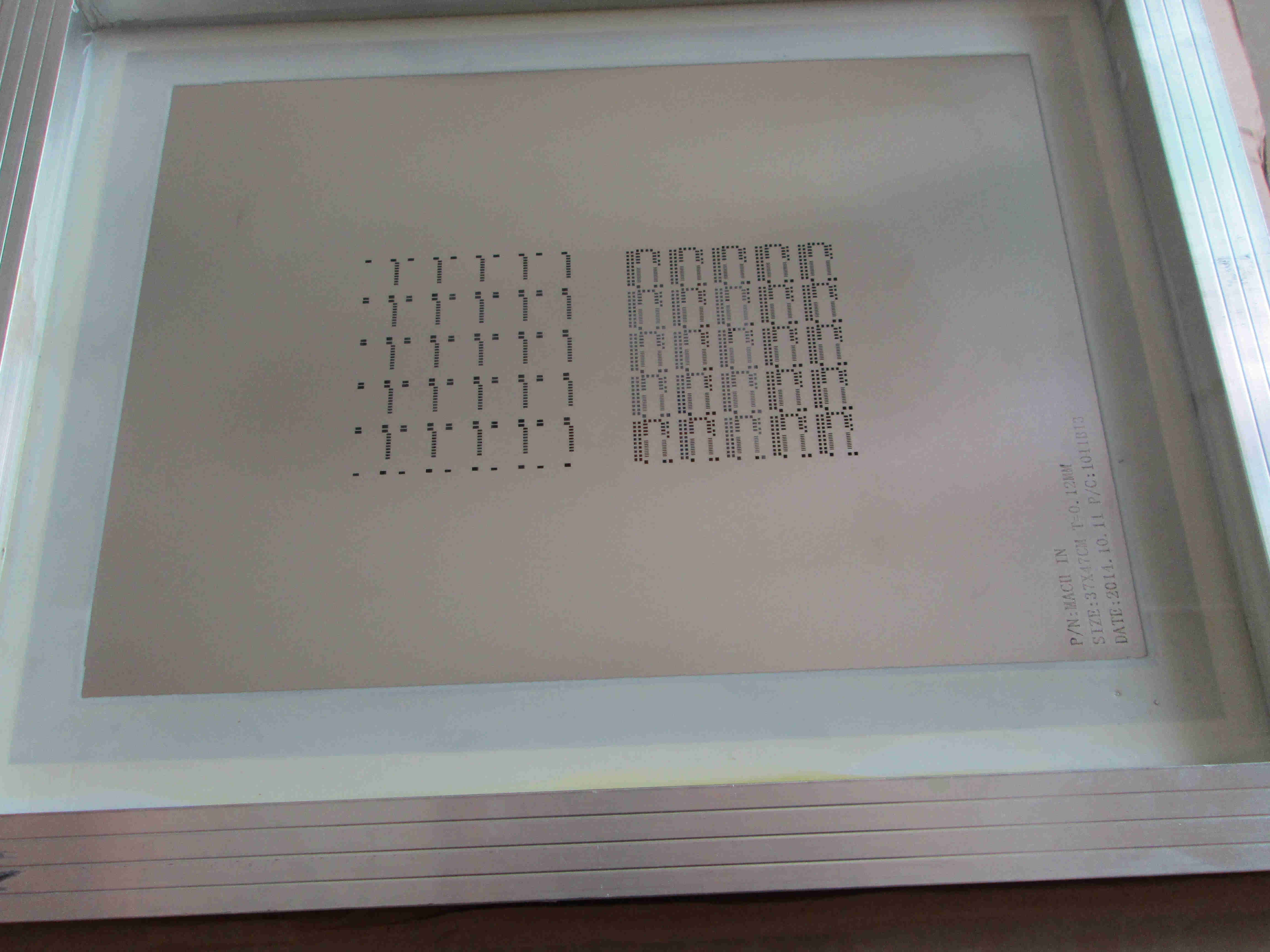
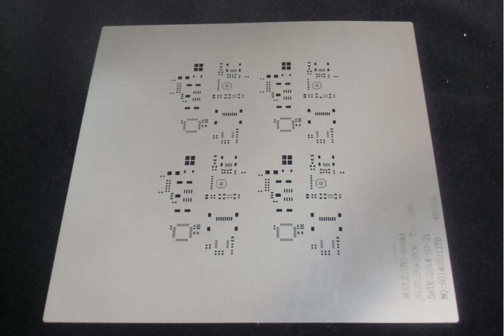
Laser Stainless Stencil (Generally called Stencil) is one important tool that used in pasting the solder tin while assembly process.
There are two kinds of stencils, one is stencil with frame, the other one is stencil without frame.
General stencils will be fabricated and shipped out in 2-3 days.
Limitation on PCB size:
Frame Dimension Effective Dimension
20cm X 20cm no frame 18.0cm x 18.0cm
20cm X 25cm no frame 18.0cm x 23.0cm
20cm X 30cm no frame 18.0cm x 28.0cm
28cm X 38cm no frame. 19.0cm x 29.0cm
30.0cm x 40.0cm 13.0cm x 21.0cm
37.0cm x 47.0cm 19.0cm x 29.0cm
42.0cm x 52.0cm 24.0cm x 34.0cm
45.0cm x 55.0cm 27.0cm x 37.0cm
58.4cm x 58.4cm 40.0cm x 40.0cm
55.0cm x 65.0cm 37.0cm x 47.0cmm
Gerber file requirement:(The following layers are needed)
Top Paste layer: pcbname.GTP
Bottom Paste layer: pcbname.GBP
Top Silk Layer: pcbname.GTO
Bottom Silk Layer: pcbname.GBO
Note:
►No limitation on panelizing.
►The Gerber file must be RS-274x format.
►If there are GBP layer and GTP layer(Bottom Paste layer and Top Paste layer), please also provide the Bottom silk screen layer. so that the stencil engineer will know whether mirror the bottom layer or not.
►We will open all the paste layer, but there are also some exception sometimes, such as standard golden fingers, standard RF antenna.
►If there isn't paste layer, but there are Solder Mask layer, Top Layer and Bottom layer. we will manufacture it according to Solder Mask layer and the size of the pads.
►The thickness of the stencil will be 0.1mm,0.12mm,0.15mm,0.18mm or 0.2mm.
►The shape of holes on the stencil for the SMT pads may a little difference from the gerber file. especially for the big pads